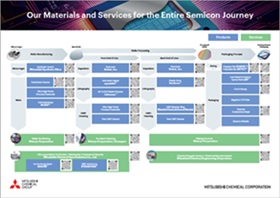
Comprehensive Semiconductor Solutions
- Language

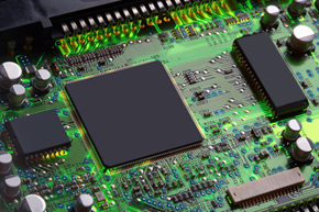
Mitsubishi Chemical delivers advanced materials and process solutions for the rapidly evolving semiconductor industry.
Through high‑purity, reliable materials and global technical collaboration aligned with our customers’ roadmaps, we help enhance performance, yield, and reliability—supporting the growth of the digital society.
Our semiconductor specialists are ready to assist. Please contact us for material selection or detailed specifications.
6products.
[Close all]
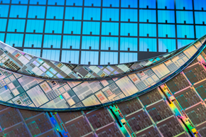
We offer ultra‑high‑purity process materials and consumables for wafer manufacturing, rigorously controlled for low metal and particle levels.
For silicon ingot and wafer production, we provide optimized materials and technologies tailored to each process—please contact us for details.
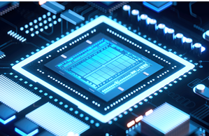
We offer proven materials solutions supporting FEOL miniaturization, including lithography, deposition and etching, as well as CMP and cleaning processes.
From our broad lineup, we deliver process‑specific materials and technologies optimized for each process and equipment requirement.
Semiconductor Solutions, Back End Of Line(BEOL)
[Close all]
We provide materials that support BEOL miniaturization and high‑density interconnects, covering CVD and ALD, lithography, CMP and cleaning, and multilayer interconnect formation.
Semiconductor Solutions, Packaging Process
[Close all]
We provide and develop materials that support high‑density packaging and long‑term reliability, covering dicing and bonding, encapsulation and adhesion, thermal management, thinning, and warpage control.
Semiconductor Solutions, Services
[Close all]
Our broad range of services—including wafer reclaim, precision cleaning, contract plating, ultra‑pure water and wastewater treatment systems, and chemical supply systems—enables us to propose solutions and technologies tailored to each customer’s production conditions and quality requirements.
Semiconductor Solutions, Power Device
[Close all]
We supply GaN substrates for power device applications.
We also develop advanced thermal management materials—including insulating heat‑dissipation sheets and low‑CTE materials—and provide solutions tailored to customer quality requirements. Please feel free to contact us for further information.
- Product Finder
-