
Semiconductor Materials
324 products.
Filter by Application
[Close]
30 products.
[Close all]
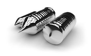
We offer ultra‑high‑purity process materials and consumables for wafer manufacturing, rigorously controlled for low metal and particle levels.
For silicon ingot and wafer production, we provide optimized materials and technologies tailored to each process—please contact us for details.
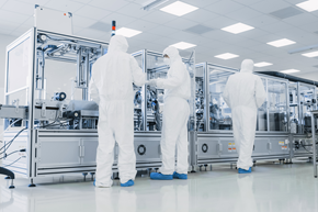
We offer proven materials solutions supporting FEOL miniaturization, including lithography, deposition and etching, as well as CMP and cleaning processes.
From our broad lineup, we deliver process‑specific materials and technologies optimized for each process and equipment requirement.
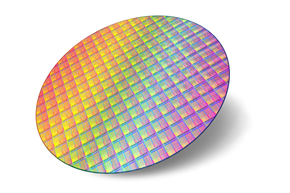
We provide materials that support BEOL miniaturization and high‑density interconnects, covering CVD and ALD, lithography, CMP and cleaning, and multilayer interconnect formation.
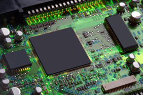
We provide and develop materials that support high‑density packaging and long‑term reliability, covering dicing and bonding, encapsulation and adhesion, thermal management, thinning, and warpage control.
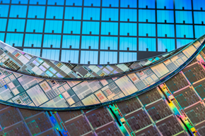
Our broad range of services—including wafer reclaim, precision cleaning, contract plating, ultra‑pure water and wastewater treatment systems, and chemical supply systems—enables us to propose solutions and technologies tailored to each customer’s production conditions and quality requirements.
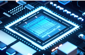
We supply GaN substrates for power device applications.
We also develop advanced thermal management materials—including insulating heat‑dissipation sheets and low‑CTE materials—and provide solutions tailored to customer quality requirements. Please feel free to contact us for further information.
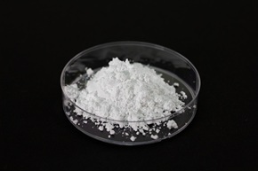
In Development
Inorganic particles with negative thermal expansion (NTE) properties. When compounded into resin materials, they significantly reduce the coefficient of thermal expansion (CTE), improving dimensional stability.
- ※M-Filleris™ is a family of functional fillers developed by Mitsubishi Chemical for semiconductor materials and advanced packaging applications.
GaN Wafer (GaN substrate)
[Close]
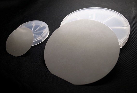
Mitsubishi Chemical's Gallium Nitride (GaN) substrate is a high-quality single-crystal substrate. It is made with original HVPE method and wafer processing technology, which has been originally developed for many years. The features are high crystalline, good uniformity, and superior surface quality. GaN substrates are used for LD applications (violet, blue and green).
Furthermore, development has progressed for power and high frequency electronic device applications. In order to achieve lower defect and higher productivity, we have been developing the GaN substrates manufactured by SCAAT™(*) and SCAAT™-LP(**).
- *SCAAT™ is the brand name of an acidic ammonothermal technology implemented by Mitsubishi Chemical Corporation. This technology was established through the cooperation of Tohoku University, The Japan Steel Works, Ltd., and Mitsubishi Chemical Corporation.
- **SCAAT™-LP is the brand name of a low pressure acidic ammonothermal technology implemented by Mitsubishi Chemical Corporation and The Japan Steel Works, Ltd. This technology was jointly developed by Tohoku University, The Japan Steel Works, Ltd., and Mitsubishi Chemical Corporation.
NEWS LETTER -Gallium nitride (GaN), a material to support future society-([PDF]465KB)
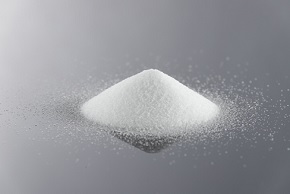
Ultrapure synthetic silica powder (7N) derived from silicon alkoxide. Ideal as a raw material for quartz glass (silica glass) which requires high purity.
- CASNo.:
- 60676-86-0
- EINECS:
- 262-373-8
This photosensitive polymer for photo resists is used during the formation of semiconductor circuits.
This material is designed to satisfy strict quality requirements, such as high purity and low metal content, associated with the miniaturization of circuit patterns.
Our services include polymer design, prototyping, and mass production.
This antistatic agent is used to prevent electrons from accumulating on the resist surface during electron beam lithography.
This material is used in advanced photomask manufacturing to help prevent charge-up failures.
Antistatic Agent, aquaPASS™
[Close]
This water-based antistatic agent is derived from polyaniline-based, water-soluble electroconductive polymers.
This agent prevents particles from adhering due to static electricity when used as a coating on films and plastic substrates.
Use of this agent enables the production of thin films with excellent antistatic performance, transparency, and minimal humidity dependency.
During the post CMP cleaning process in semiconductor manufacturing, it is important to remove organic residues and particles on Cu wires and Low-k films without damaging the substrate. Our product, MCX-SDR4, is a high-efficiency cleaning solution suited for semiconductor industries.
Characteristics:
- High efficiency particle removal
- Removes organic residues effectively
- Limits galvanic corrosion on Cu wire
- Limits Low-k damage
- Improves Low-k wetting properties
In recent years, the demand is increasing for high quality removal of metals from small size semiconductor circuits during silicon wafer cleaning process. Star Series meets this demand with semiconductor process chemicals having metal impurity levels below 10ppt.
Products: Hydrochloric acid
MC1 is an electronic chemical processing solution which is a high-performance alternative RCA clean. MC1 contributes to the customer`s total cost reduction, because it can remove both particles and metals, thus reducing the number of steps of RCA cleaning. Features: ・Reduction of metal contamination ・Prevention of cross contamination
- Product Finder
-