GaN Wafer (GaN substrate)
Mitsubishi Chemical Corporation- Language
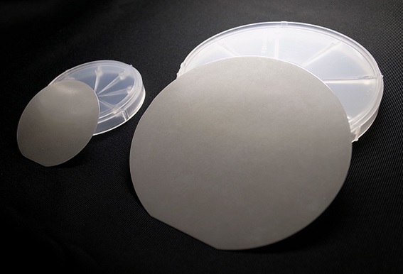
Mitsubishi Chemical's Gallium Nitride (GaN) substrate is a high-quality single-crystal substrate. It is made with original HVPE method and wafer processing technology, which has been originally developed for many years. The features are high crystalline, good uniformity, and superior surface quality. GaN substrates are used for LD applications (violet, blue and green).
Furthermore, development has progressed for power and high frequency electronic device applications. In order to achieve lower defect and higher productivity, we have been developing the GaN substrates manufactured by SCAAT™(*) and SCAAT™-LP(**).
- *SCAAT™ is the brand name of an acidic ammonothermal technology implemented by Mitsubishi Chemical Corporation. This technology was established through the cooperation of Tohoku University, The Japan Steel Works, Ltd., and Mitsubishi Chemical Corporation.
- **SCAAT™-LP is the brand name of a low pressure acidic ammonothermal technology implemented by Mitsubishi Chemical Corporation and The Japan Steel Works, Ltd. This technology was jointly developed by Tohoku University, The Japan Steel Works, Ltd., and Mitsubishi Chemical Corporation.
NEWS LETTER -Gallium nitride (GaN), a material to support future society-([PDF]465KB)
Characteristics
[Close]
- 1.Mitsubishi Chemical provides high-quality GaN substrates which are produced by originally designed HVPE (Hydride Vapor Phase Epitaxy) method, utilizing more than 30 years of experience in the GaAsP epi-wafer business.
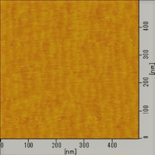
- 2.More than 30 years of wafer fabrication technology experience with GaAs substrates has been applied to the GaN substrate production. GaN substrate has a damage-free, very flat (Rms < 0.2 nm), controlled surface orientation, and controlled atomic steps surfaces. Surface quality suitable for epitaxial growth has been achieved.
- 3.In order to achieve lower defect and higher productivity, we have been developing the GaN substrates manufactured by SCAAT™ and SCAAT™-LP.
Applications
[Close]
- Laser diodes: violet LD, blue LD, and green LD
- Power electronic devices, High frequency electronic devices
Usage
[Close]
Substrates for epitaxial growth by MOCVD etc.
Inquiries Concerning Products
View the products of Semiconductor Div., Mitsubishi Chemical[Open in a new window]